[WIP] Hacking a ED060SC4 Replacement E-Ink Screen
Status of this article
This article is still being written and the project not finished. I’m taking a head start of the writing before I get too lazy to write anything.
As of 2023-04-28, I ordered the PCB and the components. Nothing has been tested
yet so wait and see ¯\_(ツ)_/¯
Introduction
My initial project idea was to take an ESP32, a wifi-capable microcontroller, and connect it to an E-Paper Display (EPD) and a battery in order to turn it into a weather display. This project is fairly simple but I discovered that EPDs were pretty expensive! For example, a 5.83inch 648x480 EPD from Waveshare costs about 46€. For this price, you’d get the display itself and a shield to drive the display via SPI.
After researching a bit, I found that some people were using a display meant to
be a replacement for some ebooks by Pocketbook: the ED060SC4. This has a good
advantage, as the display is 6” 800x600 and costs about 25€.
This method is though not plug-and-play, as it involves using specific
components and code. This includes generating several different voltages,
connecting most of the 39 pins of the display and finally writing the code that
will create the correct pulses, referred to as waveforms.
The weather display project was then put on hold and I decided I’d make a
driver board for the ED060SC4 that could be controlled via SPI, as if I had
bought something from Waveshare.
I’ve done a fair lot of C in the past and recently some Rust. As the support
for Rust on microcontrollers seems to be good and rising, I decided I would try
to write everything in Rust.
Resources
Thankfully, I didn’t have to reverse engineer the display myself as many
people already put in the hard work.
Here’s a list of the articles that helped me through this project, along
with the main reason I used them:
- EssentialScraps: Apparently the first person to reverse the display, cited by everyone. Good overall description of the project.
- Sprites Mods: Another well-cited source. Improvements on Essential Scraps’ design, as some display variants required non-connected pins to actually be connected.
- PushRAX: General hardware understanding.
- Alex Franchuk: General understanding.
- EPDiy: PCB routing.
- PaperBack: Very impressive project and clean schematics.
Hardware
I made a public Github repository with the KiCad files, where you can find the schematics, PCB and components used for the board: Github Project.
Requirements
Let’s start with the basics of what is needed to make this project work.
The ED060SC4 interfaces with a 39-pin connector. The datasheet
states the use of a JST connector 39FXL-RSM1-S-H-TB which can not be found
anymore. Thankfully, once again, several persons found that the Hirose connector
FH26W-39S-0.3SHW(60) had the same pitch and could be used as a replacement.
The ED060SC4 requires no less than 6 different voltages to work: -20V, -15V,
+15V, +22V, a regular +3.3V and a display specific VCOM usually around -1.5V.
Generating those voltages can be a bit tedious and finding something power
efficient even more. I found via EPDiy and a FPGA project
that the Texas Instruments IC TPS65185 was specifically made for E-Ink
displays requiring this kind of voltages. It is a bit pricy, about 2.4€, but
at least there’s no need to worry about efficiency and schematics are widely
available.
Next is the microcontroller. The main requirement was the number of pins as I
didn’t want to bother with multiplexers. I also needed a good support of Rust
along with easy to understand examples as it would be my first real embedded
project in Rust. I settled on the STM32F103C8T6 that is widely available,
documented and an industry standard. The development board Blue Pill is
fairly cheap and gave me the occasion to try the Rust toolchain with some
examples.
The Raspberry Pi RP2040 could also be a alternative and has the advantage of
costing only about 1€, compared to the 2€ of the STM32.
Now that everything has been roughly defined, let’s jump into the details!
Schematics
The schematics are broken into three pages to make it easier to understand:
- The board with the microcontroller and its peripherals.
- The powers rails with the
TPS65185IC. - The EPD
ED060SC4.
All the schematic pages are also available in one PDF.
Board

Some features of the STM32 MCU, like SPI and I²C can only be used on specific pins. Assigning the pins can either be done with a regular picture of the pinout or via STM32CubeMX.
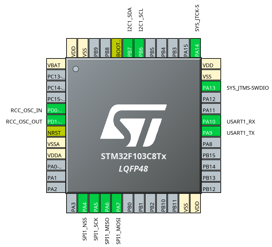 The
The TPS65185 requires 2 pins for I²C and at maximum 5 other pins.
The ED060SC4 EPD requires 8 data pins and 7 for the clock and enabling the
various registers.
The STM32 itself needs a crystal for the clock, that wil take up 2 pins.
As an interface for the user, more pins are needed: 4 for SPI, 2 for UART and
finally 2 for Serial Wire Debug to program the chip.
That is in total 32 pins. Good thing the STM32F103C8 has enough!
The choice of capacitors, crystal and VBAT filtering circuit of the STM32 was
done by following Phil’s Lab
excellent videos on the subject. In one of his latest videos he states that no
resistor is needed for the crystal. To be safe I still added a 0Ω resistor in
case I actually need it.
I chose simple standard 2.54mm connectors for the UART, SPI and SWD. I did the
same for the WAKEUP and PWRUP pins of the TPS65185 so I could power it
up externally without the STM32 in case something was fundamentally wrong with
my design. The first three connectors are connected to TVS diodes to protect
from electrostatic discharges (ESD).
All the power rails of the EPD are also wired to a connector so the TPS65185
could be used for other applications or some testing.
Power Rails

There’s a lot going on in this schematic but thankfully Texas Instruments made a great job with the TPS65185 Datasheet and its evaluation module. The schematics described in those are exactly the ones we need, as some voltages can be choosen with different resistor values.
The IC basically uses a Boost converter and a Buck-Boost converter to generate
±16V rails. Those voltages are then lowered via two LDOs to get the ±15V rails.
Two charge pumps on the other hand can boost the ±16V to -20V and +22V.
VCOM can be programatically set to output between 0V and -5.11V, and V3P3
to output or not the +3.3V input to save power by disconnecting the EPD.
VCOM_CTRL enables the VCOM amplifier when pulled high. This lets us set the
VCOM voltage before turning it on. It is not strictly required to connect it to
the MCU and can be left high with a pull-up resistor, as the datasheet states.
The WAKEUP and PWRUP pins are respectively used to turn on the programming
interface of the IC (I²C) and then the rails. The idea here is to pull WAKEUP
high, set the VCOM voltage, enable V3P3 and then pull PWRUP high.
PWRGOOD and INT are used to signal a fault, like rails that can’t be
powered up properly. Those could be ignored unless specific code is implemented
to recover from faults.
The schematics also include a temperature sensor in the form of a thermistor in parallel with a resistor, as the IC can be programmed to stop operation above a certain temperature. I will not use this feature but it doesn’t hurt to add it as the footprints and price are negligible.
The resistors R1-R2 and R8-R9are used for the feedback of the charge pumps,
to generate the adequate voltage. R6-R7 are used on the other hand to pull
high INT and PWR_GOOD that are open-drain pins.
Most capacitors are used as decoupling capacitors, the others for the charge
pumps.
The inductors L1-L2 are used by design in the boost converters.
EPD

I mainly followed PaperBack’s and Alex’s schematics to
wire the EPD.
However, as stated by Alex and before that SpritesMods, the pins 9 and 10 need to
be connected respectively to ground and +3.3V, even though they are marked NC
in the datasheet.
I included additional capacitors for the pins that would be drawing current but they’re probably not needed and can be left unpopulated.
As many pins are linked to the same nets, the 39-pin connector now turns into a less frightening 21 pins!
PCB Design
The board stackup is a standard 4-layers: signal / GND / 3.3V / signal.
An interactive BOM
generated by KiCad is available, where every net and component can be
highlited to better understand what’s going on. By default, all components are
grouped by Value and LCSC Part Number.
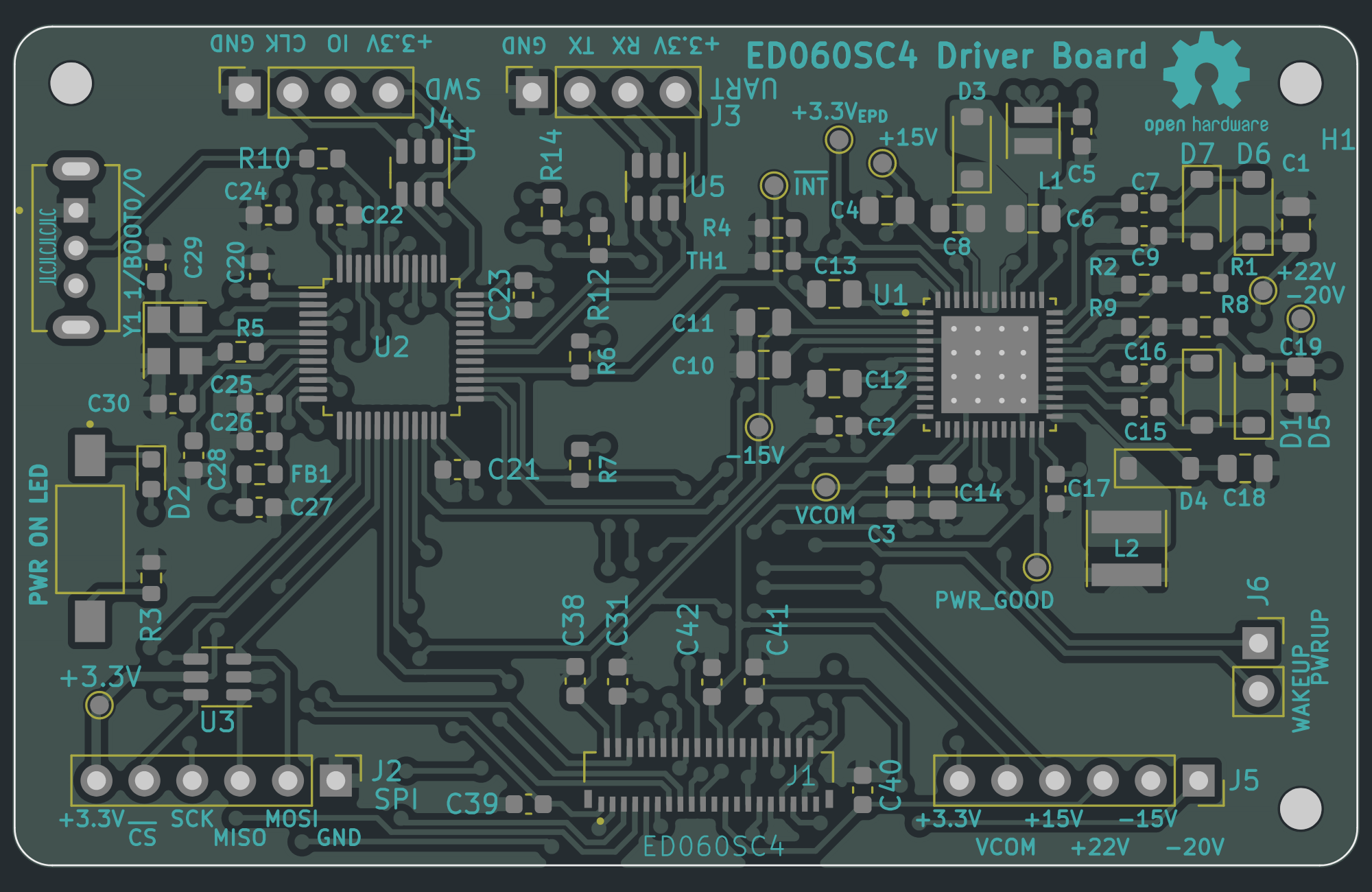
There isn’t much to say here, all the placement and recommendations come from Phil’s Lab once again. There’s always a better way to do PCB routing, but this one should be good enough. The subreddit r/PrintedCircuitBoard is also an impressive resource, especially through its Wiki and the questions people ask.
Notably though, the +3.3V pins of the various connectors have a keepout so they don’t connect to the internal +3.3V plane of the board. This is made so the current has to flow through the ESD protection chips first. Then the current goes into the power plane.
I tried selecting small components so the routing would be easy to do, but not
too small either so it could still be handsoldered. The smallest footprint is
0603 for capacitors, resistors and LED.
The TPS65185 would benefit from being soldered with hot air as the pad
underneath is used to dissipate heat.